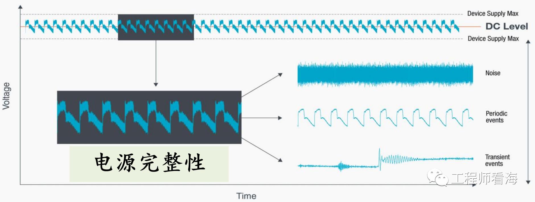
SI (Signal Integrity) focuses on the waveform quality of signals, while PI (Power Integrity) addresses the quality of power waveforms. The subject of PI research is the PDN (Power Distribution Network), which investigates power issues from a more systemic perspective. The goal is to eliminate or alleviate power noise, meet the demands of loads for different frequency currents, and provide a clean, stable, and reliable power supply for the loads. Similar to SI, PI is one of the fundamental requirements for PCB engineers, and the routing quality and performance of the PDN are critical aspects of assessment.

This section introduces Power Integrity, highlighting the differences between SI and PI. SI analysis is based on transmission lines, while PI analysis is based on power planes. Common corrective measures for SI involve modifying trace widths, lengths, and reference layers. In contrast, PI corrective methods include adjusting the routing of power/ground planes, optimizing matching capacitor values, adjusting capacitor quantities, or modifying installation methods.

In the hardware design of mobile baseband or other circuit systems, the Power Distribution Network (PDN) is likely the most intricate interconnection structure. I also recommend beginners to start with the power aspect, which encompasses two main aspects. The first involves the foundational structure of power, including BUCK, LDO, and other power architectures. A power tree can provide a basic understanding of the power requirements for various modules on a mobile device. The second aspect is the PDN, which ensures the effectiveness of the entire system, preventing voltage fluctuations beyond specifications under complex operating conditions that could lead to system anomalies. Understanding power thoroughly enables a comprehensive design from the power source to the interconnection links and ultimately to the loads. This deep understanding of power will provide an overall impression of mobile device design, enhancing comprehension of the entire hardware system. It will make handling tasks such as charging, audio, screen, camera, and sensors more manageable.
In the aforementioned two aspects, the former is the focus of power engineers, while the latter is the focus of power integrity engineers. Compared to power engineers, PDN is more concerned with power paths and terminals. The PDN link begins at the voltage regulator module (VRM) in the power module, including PCB traces, capacitors, vias, package, and die capacitors along the way. The PDN link is intricate and complex, requiring a systematic approach to analyze and optimize PDN, ultimately achieving the goal of providing a stable and clean power supply for the chip.

When designing the Power Distribution Network (PDN), attention is given to both the DC and AC components. The DC component, expressed as ∆V=∆I*R, involves the presence of series resistance from the Voltage Regulator Module (VRM) to the Integrated Circuit (IC). When a DC current flows from the VRM to the load, there is a voltage drop due to the line resistance. For instance, with a current of 1A and a line resistance of 10mΩ, an IR drop of 0.01V occurs. This drop, known as IR drop, is variable as the load current fluctuates. For instance, when the load operates at 2A, the IR drop becomes 0.02V, similar to the scenario described earlier regarding LDO routing.
However, the load does not consistently operate at a fixed current. For example, during gaming, the CPU engages in complex computations, and the GPU performs intricate rendering. The internal switches of these chips operate at high speeds, leading to a complex and time-varying current draw from the power supply. Analyzing this dynamic current draw requires the introduction of parameters related to time and frequency, namely impedance (Z, where impedance = resistance + capacitance + inductance). Voltage fluctuations are caused by fluctuations in current.
Returning to the classical formula ∆V=∆IR, with a slight modification, it becomes ∆V=∆IZ. While R is a constant independent of frequency, Z depends on frequency. ∆V represents the change in voltage caused by a change in current. If ∆V is too large, exceeding the allowable voltage fluctuation for the load, it poses a risk. Typically, loads tolerate voltage fluctuations of around 5% or 3% (specifically as per the load's manual). Therefore, voltage fluctuations should not exceed this 5% or 3%. For example, if the load requires 0.75V, assuming a maximum tolerable voltage fluctuation of 3%, it can accept a maximum fluctuation of 0.0225V. If the actual voltage fluctuation is only 0.015V, it meets the load's requirements.
Let's revisit the formula ∆V=∆I*Z and simplify it to obtain the following equation: ∆V=∆I×Z

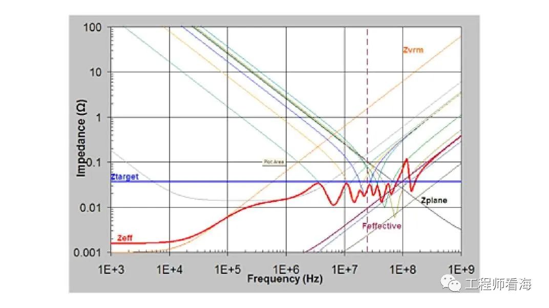
The principle behind designing the Power Distribution Network (PDN) is to optimize the impedance (Z) along the links, ensuring it is lower than the target impedance (target Z target). This ensures that the voltage can meet the requirements of the load. In essence, it involves constraining impedance to control power fluctuations. To achieve this, I need to know the target impedance and the specific models of capacitors on the line. Additionally, precise simulations are necessary to obtain a reliable design.

For example, the graph above illustrates the impedance frequency curve. If the load operates at a single frequency, assuming a sinusoidal current at a single frequency, optimizing impedance becomes straightforward—only the impedance at this frequency needs to be lower than the target impedance. However, real-world scenarios are more complex, and we may not know the specific working frequencies. To err on the side of caution, we control the impedance within a certain frequency range rather than targeting DC or a single frequency. This may seem like an over-design, but it is indeed a very safe design approach. The blue curve represents our target impedance, and our goal is to optimize the PDN impedance within this frequency band (effective frequency band) so that the actual impedance, represented by the red curve, stays below the target impedance in the load's required frequency range.
