PCB panelization is a crucial step that not only impacts production efficiency but also directly relates to product quality and cost. Well-designed panelization can optimize the manufacturing process, reduce waste, and enhance production capacity.
However, in practical applications, many engineers encounter issues with their PCB panelization due to various factors. This article will explore the rationale and importance of PCB panelization, helping you understand how to optimize panelization design, improve production efficiency, and reduce costs. Let's delve into the discussion: Is your panelization reasonable?
When is panelization necessary?
It is advisable to implement panelization design to enhance production efficiency when one side of a PCB single board is smaller than 50mm. This is because machines cannot produce boards with panel dimensions smaller than the machine's production capabilities. The maximum panelization size that Huaqiu can handle is: Single/Double-sided boards ≤ 6050cm, and Multi-layer boards ≤ 5040cm. Generally, keeping the panelization size within this range ensures a certain guarantee of surface mount efficiency.
Panelization Size
Stamp hole connection size (applicable to irregular boards): The panelization size should be greater than 50*50mm (it is recommended to panelize as large as possible for efficiency). It is crucial to note that after breaking the stamp hole panelization, there may be gear-like unevenness. V-cut size (applicable to boards with a square shape): For panelization using V-cut machines, the length and width after panelization must be at least 60mm, and the maximum size after panelization is 480mm.
It is essential to note that V-cut only follows straight lines, defaults to double-sided V-cut, and does not perform single-sided V-cut. The copper surface, traces/solder pads, and other edges should be at least 0.4mm away from the V-cut centerline to avoid copper exposure during V-cutting (Additionally, installation holes should be placed away from the V-cut line to prevent hole breakage during board separation).
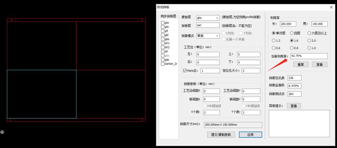
Board material utilization: The ratio of the shipped area to the total material area. The standard ratio should be above 85%, and low utilization rates can increase production costs. The recommended panelization size is around 150*200mm for optimal results. Huaqiu DFM provides a utilization calculation function, automatically determining the panelization material utilization after completion.
Process Edge Requirements
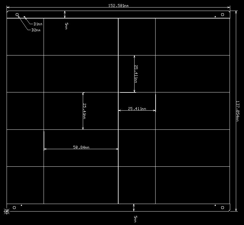
The standard width for process edges is typically 5mm (minimum 3mm), with the addition of four locating holes, each having a diameter of 2mm (without copper plating). Additionally, four asymmetrically distributed solder mask-defined pads with a diameter of 1mm (with a 2mm opening in the solder mask) are included.
When components on the PCB are within 5mm of the board edge and SMT rails are required for assembly, an additional 5mm of double-sided process edge is conventionally added to facilitate assembly within the rails. For wave soldering processes, components should be positioned at a distance greater than 5mm from the board edge.
Consistent Panelization Orientation
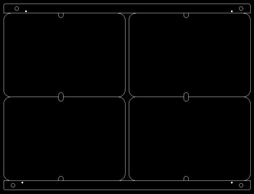
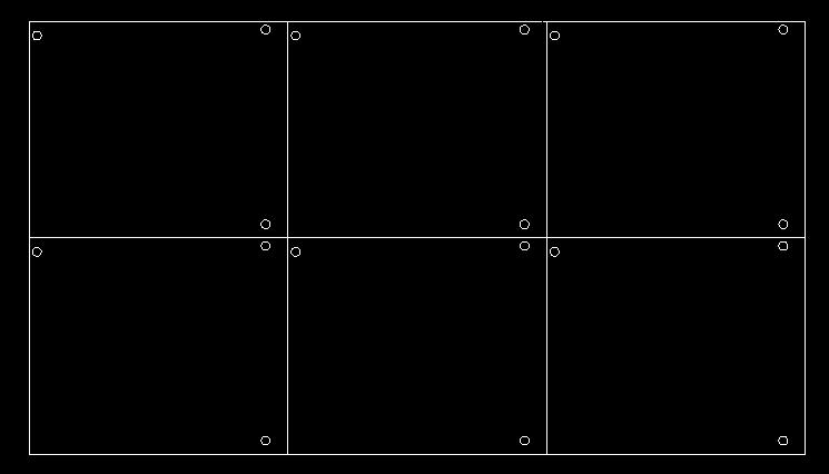
For boards with a more regular outline, it is advisable to maintain a consistent orientation of individual panels during panelization. This facilitates the operation of pick-and-place machines or manual assembly.
CNC + V-CUT Panelization
Combining milling (CNC) with V-cut panelization is suitable for boards with components near the board edges, preventing panelization without spacing. This involves milling the edges with a CNC process, applying V-cut treatment at both ends, and creating milled gaps in the middle to facilitate the soldering of components. Without this approach, interference between components near the board edges may occur, making assembly and soldering difficult.
Stamp Hole Bridging in Panelization
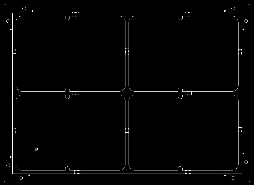
Stamp hole bridging is a panelization method, and it can address issues that V-CUT bridging cannot solve. For instance, it is suitable for circular boards or irregularly shaped boards where V-CUT is not applicable; in such cases, stamp hole bridging is the only viable connection method.
V-CUT Bridging in Panelization
V-CUT bridging in panelization is suitable for regular-shaped boards. Since the V-CUT blade cannot make turns, the V-CUT positions must be in a straight line. It is important to note that when components are positioned near the board edge, V-CUT should not be used, as it may impact assembly and soldering processes.
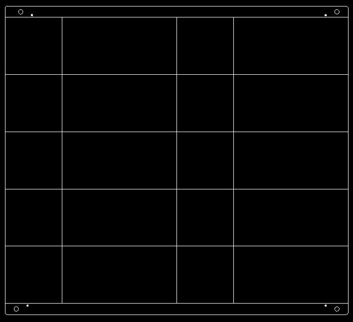
Panelization without Process Edges
To maximize material utilization, panelization without process edges can be adopted. To ensure ease of production and assembly, the panel must include locating holes and mark points. Additionally, the distance from the mounting position to the board edge should be greater than 5mm to avoid the need for special fixtures during assembly soldering, which would impact costs.
Interference in Panelized Components
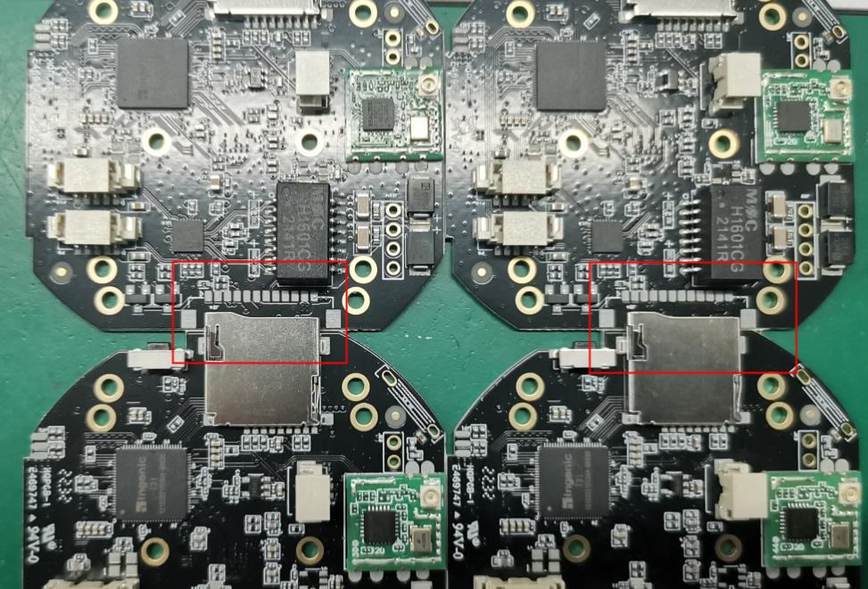
Peripheral connectors, including USB, TYPE-C, HDMI sockets, TF card sockets, SIM card sockets, micro USB, headphone jacks, RF connectors, optical fiber cages, DC sockets, MINI USB, as well as audio and video jacks, require careful consideration in panelization. Especially when these components extend beyond the board edges, it is crucial to maintain appropriate spacing during panelization to prevent interference with devices on other panels, ensuring proper component assembly. See the diagram below:
Adding Substrate, Adding Stamp Holes
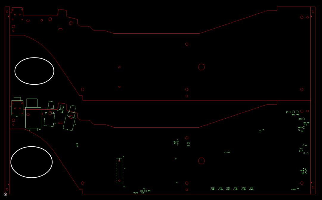
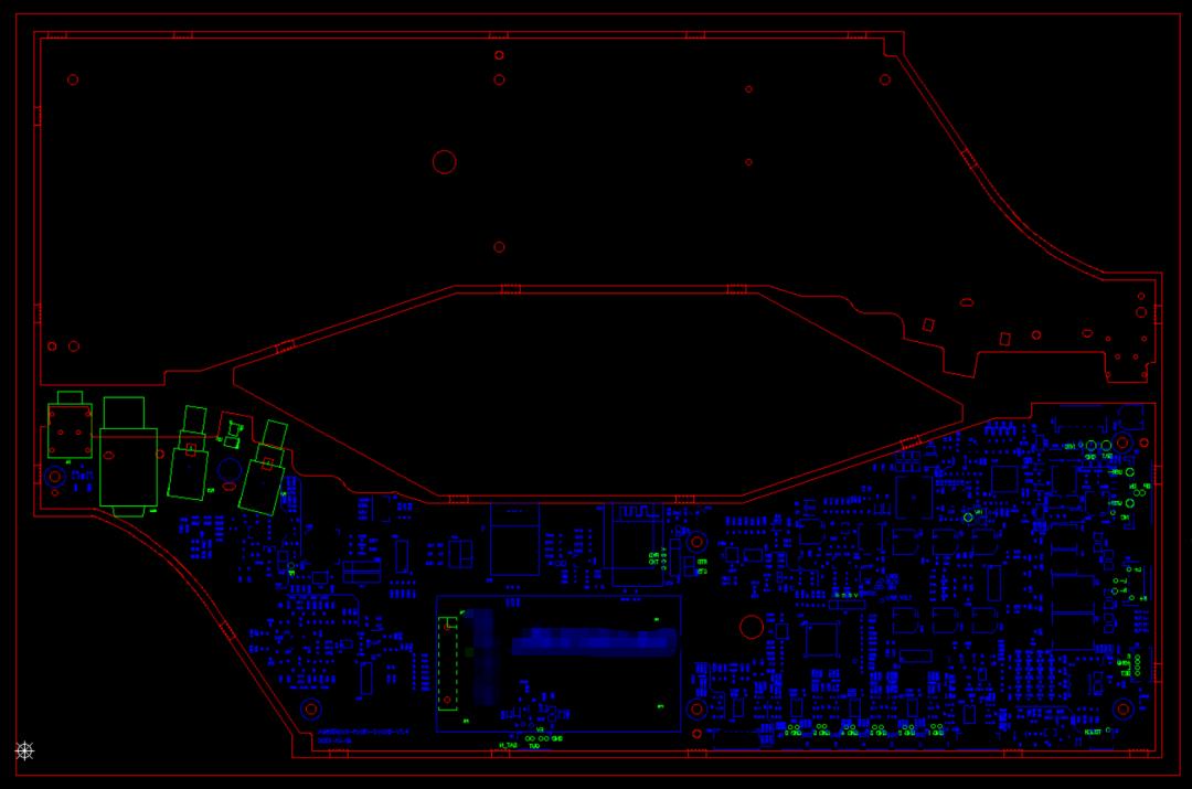
When dealing with irregularly shaped panelization, the board is susceptible to breakage due to fewer process edge connections. During wave soldering, there may be excessive solder and board deformation. To address these issues, a sub-panel can be added in the milled gap, and the PCB can be connected to the sub-panel using stamp holes. This approach effectively prevents PCB breakage, excessive wave solder, and board deformation. See the diagram below:
Spacing Must Be Maintained for Half-Holes
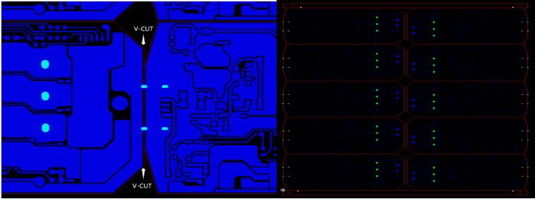
When panelizing boards with half-holes, it is crucial to leave an appropriate spacing. This is because, during the drilling process, the lack of spacing may result in damage to adjacent boards. Additionally, panelizing without spacing for V-CUT shaping can also damage half-holes, potentially tearing the copper foil within the half-holes. Therefore, to ensure the integrity and reliability of boards with half-holes, it is essential to adhere to the spacing requirements during panelization. See the diagram below:
Irregularities in V-CUT Blade Entry
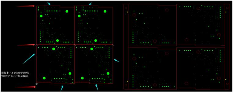
When dealing with boards with uneven outline shapes, it is essential to leave spacing for panelization if the outline is not even. V-CUT processing should not be applied in cases where the outline is uneven. Without spacing for panelization, uneven outlines cannot be V-CUT. If the uneven side faces outward during panelization, the rails cannot grip, leading to V-CUT deviations. To ensure machining quality and precision, it is crucial to adhere to appropriate spacing and panelization directions. See the diagram below:
Summary
This article has explored the rationale and importance of PCB panelization, presenting methods and techniques to optimize panelization design. By delving into the fundamental requirements, connection methods, and techniques for panelization, readers can gain a better understanding of how to optimize panelization design, enhance production efficiency, and reduce costs.
