EN
EN

The three main PCB assembly techniques are surface-mount technology, through-hole technology and mixed-technology assembly. Surface-mount technology places components directly onto PCB pads, through-hole technology inserts component leads into drilled holes, and mixed assembly combines both methods on the same circuit board.
The right technique depends on component packaging, board density, mechanical loading, power requirements, production volume, inspection access and repair expectations. Many modern electronic products use mixed assembly because a single board may contain fine-pitch integrated circuits, small passive components, large connectors, transformers and mechanically loaded terminals.
This guide explains how each PCB assembly method works, where it is most suitable and what OEM engineers should evaluate before releasing a design for production.
Reviewed by: GreensTone Engineering Team
Last updated: September 2026
PCB assembly is the process of mounting and soldering electronic components onto a fabricated printed circuit board to create a printed circuit board assembly, or PCBA.
PCB fabrication and PCB assembly are separate manufacturing stages. Fabrication produces the bare board with copper conductors, drilled holes, solder mask and surface finish. Assembly adds resistors, capacitors, integrated circuits, connectors, transformers and other components required for the board to perform its intended function.
A typical PCB assembly process may involve:
Solder paste printing for surface-mounted components;
Automated or manual component placement;
Reflow, wave, selective or hand soldering;
Cleaning when required by the approved process;
Visual, optical or X-ray inspection;
Electrical, in-circuit or functional testing;
Programming, conformal coating and final quality inspection.
The exact sequence changes according to the selected assembly technique and the component layout on each side of the board.
The main PCB assembly techniques are SMT for components mounted on the PCB surface, THT for leaded components inserted into holes, and mixed technology for boards containing both component types.
Surface-mount technology, or SMT, mounts electronic components directly onto copper pads on the surface of a printed circuit board. These components are called surface-mount devices, or SMDs.
A standard SMT process normally begins with solder paste printing. A stencil deposits controlled amounts of solder paste onto the PCB pads. Automated pick-and-place machines then position components according to the centroid or pick-and-place data supplied with the project.
The populated board passes through a reflow oven, where a controlled thermal profile heats the solder paste and forms the solder joints. The board can then be inspected using automated optical inspection. Packages with hidden connections, including BGA and some bottom-terminated components, may require X-ray inspection.
SMT supports high component density, automated placement and components on one or both sides of a board. It is widely used for passive packages, integrated circuits, QFN, QFP, BGA, connectors and other surface-mounted components.
OEM projects involving compact boards, fine-pitch devices or automated production can review GreensTone’s SMT PCB assembly in China capabilities. Current published capabilities include component packages down to 01005 and BGA packages with pitches down to 0.25 mm.
PCB and stencil verification;
Solder paste printing;
Solder paste inspection when specified;
Automated component placement;
First-article verification;
Reflow soldering;
AOI and X-ray inspection as applicable;
Electrical or functional testing.
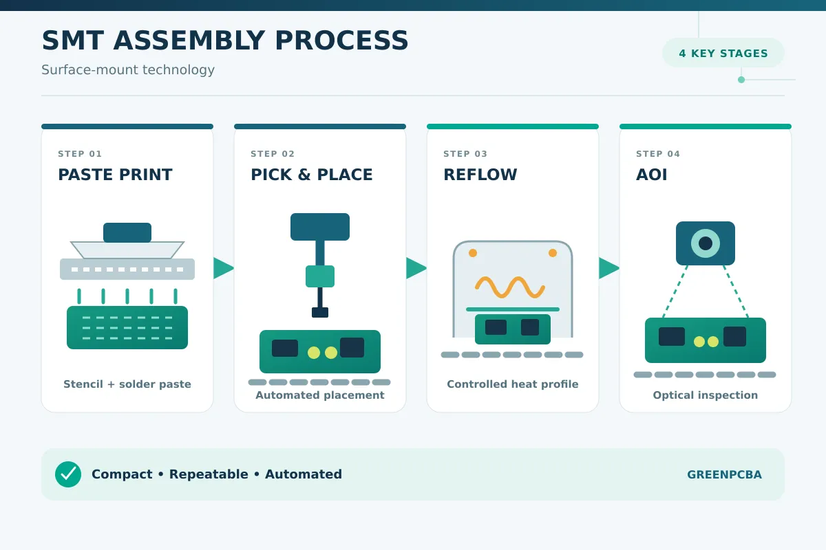
SMT is generally suitable when the product requires compact dimensions, high routing density, automated production or access to modern surface-mount component packages. It is common in communication equipment, smart meters, control systems, security products, consumer electronics and new-energy equipment.
Successful SMT production depends on more than package size. Pad design, stencil aperture, component orientation, PCB flatness, placement accuracy and the reflow profile can all affect solder-joint quality.
Through-hole technology, also called THT or plated through-hole assembly, inserts component leads into drilled and plated holes in the PCB. The leads are soldered on the opposite side of the board or within the plated barrel.
Through-hole components may be inserted manually or using automated equipment. Soldering can be completed by wave soldering, selective soldering or hand soldering, depending on board layout, production volume, component sensitivity and accessibility.
Because the component leads pass through the board, through-hole assembly can provide additional mechanical retention for large, heavy or repeatedly loaded components. Connectors, terminal blocks, switches, transformers, relays, electrolytic capacitors and some power components commonly use through-hole mounting.
GreensTone provides through-hole PCB assembly in China for single-sided, double-sided and multilayer boards, including low- and medium-volume production and mixed SMT/THT projects.
Component and polarity verification;
Manual or automated lead insertion;
Lead forming or clinching when required;
Wave, selective or hand soldering;
Lead trimming where applicable;
Visual inspection of solder wetting and hole fill;
Electrical and functional testing.
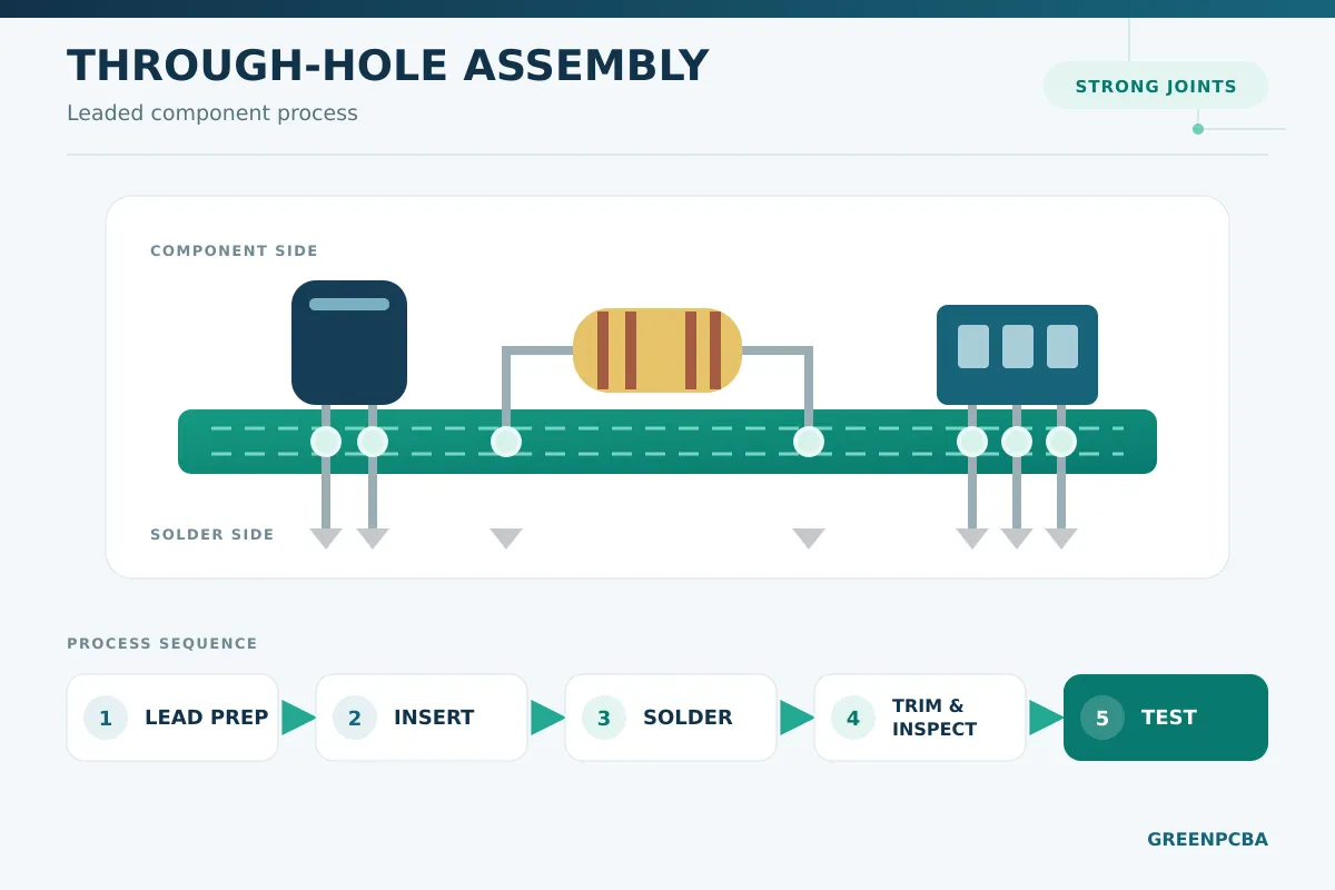
Through-hole assembly is suitable for components exposed to mechanical force, repeated mating cycles, higher power or physical loads that require stronger board retention. It is also used when suitable components are available only in leaded packages.
THT should not automatically be selected for an entire PCB simply because a product operates in a demanding environment. Many reliable industrial products use SMT for smaller electronic components and THT only for connectors, transformers and mechanically loaded parts.
Mixed-technology PCB assembly combines surface-mounted and through-hole components on the same printed circuit board. It is frequently the most practical approach for industrial and commercial electronic products.
A mixed board may use SMT for integrated circuits and small passive devices while using through-hole mounting for terminal blocks, connectors, power components or transformers. The challenge is defining an assembly sequence that protects previously soldered components and allows access for inspection and rework.
A common mixed-assembly sequence is:
Apply solder paste and place SMT components on the first side;
Complete first-side reflow;
Repeat placement and reflow for the second side if required;
Insert through-hole components;
Use wave, selective or hand soldering for the leaded parts;
Perform inspection, electrical testing and functional testing.
Component height, thermal sensitivity and clearance around through-hole leads must be considered during process planning. Selective soldering may be preferable when a board contains bottom-side SMT components that cannot be exposed safely to a full wave-soldering process.
No single PCB assembly technique is best for every product; the correct choice is the method that matches the component packages, mechanical requirements, production volume and inspection plan.
| Comparison Factor | SMT Assembly | Through-Hole Assembly | Mixed Assembly |
|---|---|---|---|
| Component Position | Mounted directly onto PCB surface pads | Leads inserted into drilled and plated holes | Uses both surface pads and plated holes |
| Typical Components | Small passives, ICs, QFN, QFP and BGA | Connectors, relays, transformers and terminal blocks | Compact electronics combined with mechanically loaded or power components |
| Primary Soldering Method | Reflow soldering | Wave, selective or hand soldering | Reflow followed by an appropriate THT soldering process |
| Board Density | Supports high component density and small packages | Requires drilled holes and generally more board area | Balances board density with mechanical component requirements |
| Automation | Highly compatible with automated placement | Automation depends on component type and volume | Requires coordination of multiple assembly processes |
| Mechanical Retention | Depends on pad, package and joint design | Leads passing through the PCB can provide additional retention | Allows stronger mounting where needed without using THT for every component |
| Inspection | AOI for visible joints; X-ray for hidden connections | Visual inspection of leads, wetting and hole fill | Requires inspection criteria for both SMT and THT joints |
| Typical Use | Compact, high-density and automated electronic assemblies | Power, mechanical, legacy and connector-heavy applications | Industrial controls, metering, power equipment and complex commercial products |
SMT may reduce board size and support faster automated placement. Through-hole mounting can provide better physical retention for certain components. Mixed technology allows engineers to apply each method where it creates the most value.
The board uses fine-pitch or high-density components;
Compact product dimensions are important;
Automated placement is practical for the planned volume;
Most components are available in surface-mount packages;
The design provides appropriate inspection and test access.
Components will experience mechanical force or repeated mating;
Large connectors, transformers or terminal blocks are required;
The selected components are available only in leaded packages;
Higher-current or physically large parts require additional board retention;
Manual modification or replacement is an important lifecycle requirement.
The product contains both compact electronic circuits and larger mechanical components;
SMT is suitable for most components but selected parts require through-hole mounting;
The PCB must balance size, manufacturability, durability and component availability;
The manufacturer can plan separate reflow and through-hole soldering stages.
The correct PCB assembly method is determined by the complete product design rather than by component size or production cost alone. OEM engineers should evaluate the following factors during design review.
The BOM may already determine part of the assembly strategy. Modern integrated circuits and small passive components are commonly supplied as SMDs, while some high-power devices, connectors and transformers remain available in through-hole packages.
Availability should be reviewed before layout release. Replacing a component package after the PCB has been designed can require footprint, stencil, panelization and enclosure changes.
Connectors subjected to repeated insertion, switches operated by users and heavy components exposed to vibration may need additional mechanical support. Through-hole leads, mounting hardware, adhesive or enclosure-based support can be considered according to the load.
Environmental reliability also depends on PCB material, solder alloy, joint geometry, component weight, thermal cycling and enclosure design. Assembly technology alone does not determine product reliability.
High-current components may require larger copper areas, wider conductors, thermal vias, heat sinks or mechanically secure mounting. The assembly method must provide enough clearance for soldering, inspection and heat dissipation.
Automated SMT normally becomes more efficient when production volume justifies stencil preparation, machine programming and line setup. High-mix, low-volume products can still use SMT, although setup frequency, feeder preparation and first-article verification must be included in the production plan.
Through-hole and mixed assembly may require more manual work. Selective soldering or dedicated fixtures can improve repeatability when recurring volume justifies the tooling.
Component placement should allow inspection of polarity, solder joints and critical mechanical features. The PCB should also include suitable test points if flying-probe or in-circuit testing is required.
BGA solder joints are hidden beneath the package, so X-ray inspection may be included. AOI is effective for many visible SMT features, while visual inspection remains important for through-hole solder wetting, lead condition and hole fill.
Products expected to remain in service for many years may require accessible connectors, replaceable modules or repair procedures. Component obsolescence should also be considered, especially for industrial products with long production lifecycles.
PCB assembly inspection evaluates materials and workmanship, while electrical and functional testing verifies connectivity and product behavior. An effective quality plan selects methods according to the defects that must be detected.
| Inspection or Test Method | Primary Purpose | Typical Application |
|---|---|---|
| Incoming Quality Control | Verify materials, part numbers, quantities and visible condition | PCB, component and mechanical-part receipt |
| Solder Paste Inspection | Measure solder paste position, area, height or volume | SMT process control before component placement |
| Automated Optical Inspection | Inspect visible component placement and solder-joint features | SMT assemblies with accessible joints |
| X-Ray Inspection | Evaluate hidden solder joints, voiding and possible bridging | BGA, QFN and other bottom-terminated packages |
| Visual Inspection | Check orientation, workmanship, wetting, lead condition and hole fill | Through-hole, mixed and manually soldered assemblies |
| Flying-Probe or In-Circuit Test | Identify selected open, short, component or network faults | Board-level electrical verification |
| Functional Test | Verify that the assembly performs defined product functions | Programmed PCBAs, modules and finished products |
Acceptance criteria should be agreed before production. Buyers can refer to the official information covering IPC-A-610 and IPC J-STD-001 when establishing workmanship and soldering requirements.
The IEC 61191-1 standard also addresses requirements for soldered electrical and electronic assemblies using surface-mount and related technologies.
High-reliability programs may impose additional workmanship controls. For example, NASA-STD-8739.3 defines soldered electrical connection requirements for applicable NASA hardware. Such standards should be used only when required by the product, customer or regulated program.
GreensTone supports SMT, through-hole and mixed-technology PCB assembly for prototype, low-volume, high-mix and recurring OEM production.
Current published capabilities include a facility of approximately 5,000 m², three SMT lines, two DIP or through-hole lines, placement of components down to 01005 and BGA assembly down to 0.25 mm pitch.
Available production and quality-control processes include:
Single- and double-sided SMT assembly;
Manual and automated through-hole insertion;
Mixed SMT and through-hole production;
AOI and X-ray inspection;
Flying-probe, ICT and functional testing options;
Component sourcing and approved-substitution control;
Firmware programming and conformal coating;
Prototype, low-volume and recurring production support.
OEM buyers can submit their Gerber files, BOM, pick-and-place data, assembly drawings, test requirements and expected quantities for a manufacturability review. GreensTone’s PCB assembly services can then be matched to the component packages, board structure, quality requirements and production stage of the project.
SMT, through-hole and mixed technology each solve different manufacturing and product-design requirements. SMT supports compact layouts and automated placement, while through-hole assembly provides additional retention for selected leaded components. Mixed technology combines both methods and is widely used when a product contains fine-pitch electronics together with connectors, transformers or power components.
The final decision should consider the BOM, PCB layout, mechanical loads, operating environment, production volume, soldering sequence, inspection access and test strategy. Reviewing these factors before production reduces redesign, assembly defects and avoidable tooling changes.
The three main techniques are surface-mount technology, through-hole technology and mixed-technology assembly. Mixed assembly combines SMT and through-hole components on the same PCB.
SMT is the manufacturing technology used to mount components directly onto PCB surfaces. SMD refers to the individual surface-mount device installed using that technology.
Through-hole leads can provide additional mechanical retention for selected components, but total reliability depends on pad and hole design, solder-joint quality, component weight, thermal cycling, vibration and enclosure support. SMT can also provide reliable performance when properly designed and manufactured.
Yes. Mixed-technology assembly is common in industrial, metering, power and control products. SMT is normally completed first, followed by through-hole insertion and wave, selective or hand soldering.
The best method depends on the final product design. SMT is suitable for prototypes using production-intent SMD packages, while through-hole parts can simplify some manual modifications. A prototype should represent the intended production design closely enough to validate manufacturing and testing risks.
A manufacturer normally needs Gerber files, a BOM with manufacturer part numbers, pick-and-place data, assembly drawings, PCB specifications, expected quantities and testing requirements. Firmware and programming instructions are also required when the PCBA must be programmed before delivery.