EN
EN

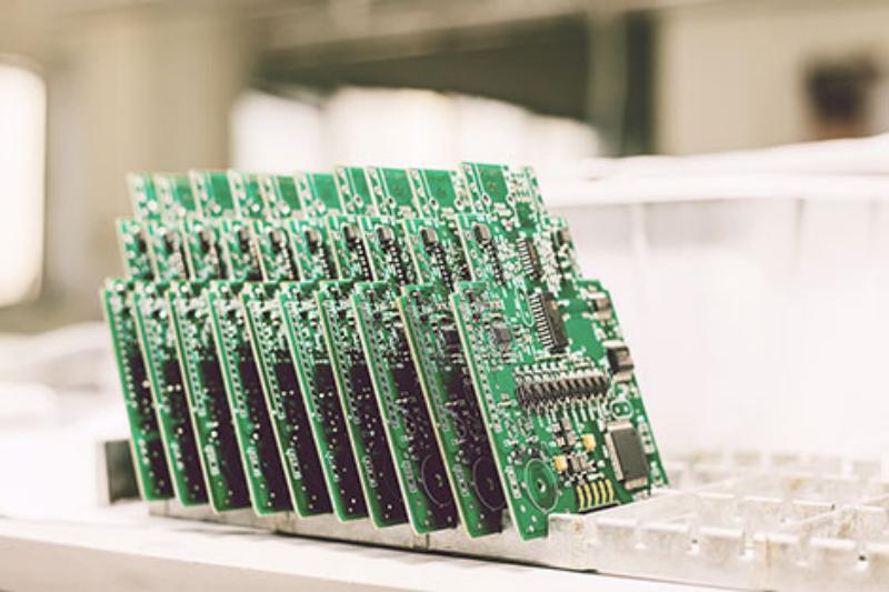
Reliable telecom pcb assembly requires precise control of signal integrity, thermal performance, component reliability, and manufacturing consistency. Unlike standard electronic products, telecom equipment often operates continuously with high data rates, strict uptime requirements, and long service lifecycles.
A qualified PCB assembly partner should evaluate not only soldering quality but also high-speed design requirements, power distribution, heat dissipation, component lifecycle risks, and production traceability. For telecom applications, manufacturing quality directly affects network stability and long-term field reliability.
Telecom PCB assembly requires advanced manufacturing control for high-speed signals, thermal management, component reliability, and long-term operation. A professional supplier must manage controlled impedance, PCB material selection, assembly process stability, inspection coverage, and traceability to ensure reliable performance in communication systems.
Telecom PCBAs are commonly used in:
Network switches
Optical communication equipment
Base stations
Routers and gateways
Data transmission systems
Industrial communication devices
These products require consistent performance because failures can affect network availability and service continuity.
Telecom equipment typically runs 24/7, creating higher demands compared with consumer electronics.
Key challenges include:
Continuous electrical loading
High-speed signal transmission
Dense component placement
High power consumption
Extended operating lifespan
A reliable electronic pcb assembly process must consider the entire product lifecycle, from prototype validation to long-term production support.
Manufacturers supporting telecom applications need strong process control because even small defects, such as poor solder joints or signal interference, can result in system instability after deployment.
Before production begins, an experienced manufacturing partner should review PCB design data to identify potential assembly and reliability risks.
High-speed telecom designs require careful control of signal transmission characteristics.
Manufacturers should review:
PCB layer stack-up
Controlled impedance requirements
Differential pair routing
Signal return paths
Trace spacing and geometry
Material dielectric properties
Poor signal integrity can lead to:
Signal loss
Crosstalk
Timing errors
Communication instability
A professional pcb assembly service china provider should collaborate with engineering teams early to verify that PCB designs are manufacturable and suitable for high-frequency applications.
Telecom systems often contain high-performance processors, communication chips, and power modules that generate significant heat.
Thermal design review should include:
Power plane design
Copper thickness
Thermal vias
Heat sink interfaces
Component placement strategy
A well-designed thermal path helps prevent overheating, performance degradation, and premature component failure.
During pcb manufacturing and assembly china, manufacturers must ensure that assembly processes maintain the intended thermal performance of the PCB design.
Telecom products often require long-term supply availability.
Component management should include:
Lifecycle status review
Manufacturer availability
Approved alternative components
Obsolescence planning
Supply risk evaluation
Using alternative parts without technical approval can affect electrical performance, firmware compatibility, or product certification.
Sensitive telecom components require strict handling procedures.
Manufacturers should control:
Moisture-sensitive device (MSD) storage
Temperature and humidity conditions
Electrostatic discharge (ESD) protection
Component shelf-life monitoring
Improper storage can cause hidden defects, especially with advanced semiconductor packages used in communication equipment.
Reliable assembly requires optimized manufacturing parameters.
Key process controls include:
Solder paste inspection (SPI)
Reflow profile verification
Placement accuracy monitoring
AOI inspection
Solder joint evaluation
For high-density telecom PCBAs, workmanship standards should be clearly defined and supported by inspection records.
An experienced pcb assembly service china supplier should provide production evidence to demonstrate process stability rather than relying only on final visual inspection.
Depending on the operating environment, telecom products may require additional protection.
Manufacturing considerations include:
Flux residue control
PCB cleaning process
Conformal coating application
Coating coverage inspection
These processes improve resistance against moisture, contamination, and environmental stress.
A reliable quality strategy uses different inspection methods for different defect risks.
Typical inspection coverage includes:
| Risk | Recommended Inspection |
|---|---|
| Solder defects | AOI, X-ray inspection |
| Hidden BGA issues | X-ray testing |
| Signal-related issues | Electrical testing |
| Component placement errors | SPI and AOI |
| Assembly failures | Functional testing |
No single inspection method can identify every possible failure mode. A combination of inspections provides stronger quality assurance.
Telecom equipment requires functional verification beyond basic electrical testing.
Testing may include:
Power-on validation
Firmware programming
Ethernet communication testing
Optical interface verification
Network protocol testing
Input/output validation
A complete testing strategy should reflect the actual operating conditions of the final product.
Some telecom applications require additional reliability validation.
Possible tests include:
Temperature cycling
Burn-in testing
Power cycling
Vibration testing
Humidity testing
These tests help identify early failures before products enter the field.
A reliable telecom manufacturing process requires complete documentation from prototype builds to mass production.
Important records include:
BOM revision history
PCB fabrication data
Assembly instructions
Inspection results
Test records
Component lot information
Production history
Traceability enables faster root cause analysis when quality issues occur.
For telecom customers, selecting a supplier experienced in pcb manufacturing and assembly china provides advantages in production scalability, supply chain coordination, and manufacturing documentation control.
A mature manufacturing partner should support:
Prototype assembly
Engineering changes
Pilot production
Volume manufacturing
Long-term product support
To receive an accurate quotation, customers should provide complete technical information.
A typical RFQ package should include:
PCB Gerber files
PCB stack-up information
Bill of Materials (BOM)
Pick-and-place files
Assembly drawings
Controlled impedance requirements
Testing requirements
Annual production volume
Packaging requirements
Regulatory specifications
Providing complete data helps manufacturers evaluate process requirements, production costs, and potential risks before starting the project.
A capable supplier can also provide engineering feedback during the quotation stage to improve manufacturability and reduce production issues.
A supplier usually needs the BOM, Gerber files, assembly drawings, pick-and-place files, testing requirements, and production forecast.
Controlled impedance is verified through PCB design review, material evaluation, test coupons, and impedance testing during manufacturing.
High-TG materials are commonly used when telecom products require improved thermal stability, reliability, or long operating temperatures.
Yes. Many suppliers can provide complete electronic pcb assembly, including PCB assembly, testing, cable integration, and final product assembly.
Choosing the right partner for telecom pcb assembly requires evaluating engineering capability, manufacturing control, testing methods, and long-term reliability support. A professional PCB assembly provider helps telecom companies reduce production risks and deliver stable communication products from prototype development to full-scale manufacturing.